Dr Surjit Singh Bhatti (Retd) Prof & Head, Physics and Dean Faculty of Sciences, Guru Nanak Dev University, Amritsar
The American Scientist Thomas Edison’s inventions of the Improved Telegraph and Telephonic systems, Phonograph, Incandescent Light Bulb, Alkaline Storage Batteries and Motion-Picture Cameras are the harbingers of today’s world. He had acquired a record number of about 1100 Patents in the last century. Dr Gurtej Singh Sandhu is one such Sikh Physicist and Engineer who today has 1325 Patents (and counting). These have ushered a revolution in the field of Computer Technology in the present century. “Technology has to be (either) invented or adopted”, Jared Diamond, the popular American Science Writer had said. Gurtej decided to invent, instead of adopting (what others had invented).

Gurtej was born on the 24th of October 1960 when his parents Dr Sarjit Singh Sandhu and Dr Gurmit Kaur were doing their PhDs in Chemistry at the University of London. He studied at London and later at Khalsa College, Amritsar, India. Thereafter he joined Guru Nanak Dev University, Amritsar, and got BSc Honors in 1982 and MSc Honors in 1983, specializing in Physics. He then went to Indian Institute of Technology (IIT) Delhi where he obtained MSc degree in 1985 in Electrical Engineering. In 1990, he earned PhD degree in Physics from the University of North Carolina, Chapel Hill, USA.
Dr Gurtej Singh Sandhu: A Prolific Inventor
Dr Gurtej Sandhu started his career in 1991 at Micron Technologies Ltd, Idaho, in USA. His research was directed to invent new IC chips for Memory Devices. He is today the Fifth Highest and the Youngest Inventor of the World. At Micron he designed the roadmap for end-to-end (Si-to-Package) in IC Technology. This included driving cross-functional alignment across various departments to identify technology gaps and develop innovative solutions for future memory scaling. At Micron he worked in the fields of Thin Film Processing and Materials, Semiconductor Device Fabrication, Very Large-Scale Integration (VLSI) and Chemical Vapor Deposition (CVD) process to produce high quality, high-performance thin films from solid state materials. His other activities included leading several project teams and driving cutting-edge research consortia around the world. He is also mentoring Engineering Majors and Faculty at Boise State University, (USA), in addition to running joint research projects with them.
New Technologies developed by Dr. Gurtej Singh Sandhu
Dr Gurtej Sandhu developed MOCVD TiN (Titanium Nitride) process, demonstrated its yield and backend reliability on 0.25-micron (a micron is one millionth of a meter) DRAM chips, which amounted to multimillion-dollar savings per year. He conceived and developed this process and implemented it into IC Manufacturing. In this method, microchips are coated without exposing the metal to oxygen, which would ruin the chips. This helped Scale the CMOS Memory Chips to sub-100 nm regimes. It is now used by device manufacturers in a $200 Billion-dollar industry.
MOCVD (Metal Organic Chemical Vapor Deposition) process is used to deposit very thin layers of atoms, at high temperatures, onto a semiconductor wafer or a substrate, which is a thin disc of sapphire or silicon. The aim is to produce a single or polycrystalline thin film. In MOCVD-TiN, a thin layer of Titanium Nitride vapor is deposited on the substrate at 300 to 400 degrees Celsius.
Recognition of Dr Gurtej Singh Sandhu’s Work (2018)
Dr. Gurtej Sandhu is a Fellow of the Institute of Electrical and Electronics Engineers (IEEE), the World’s largest technical professional organization. In 2018, he received the coveted Andrew S. Grove Award, named after the Co-founder of Intel Corporation. IEEE recognized his contributions to silicon ( s ) Complementary Metal Oxide Semiconductor (s-CMOS) process technology. CMOS enables Dynamic Random-Access Memory (DRAM) used in Computers. It is 100 times faster type of Random-Access Memory (RAM) and it stores each bit of data in a separate tiny capacitor in an IC chip. This technology is used also in NAND memory chip scaling. DRAM is 1000 times faster than NAND, though it is non-volatile and can retain data even if power is not available.
Andrew S Grove Award (Citation)
The Award recognized his “Pioneering achievements concerning patterning and material integration which have enabled the continuation of Moore’s Law for aggressive scaling of memory chips integral to consumer electronics products such as cell phones, digital cameras and solid-state drives for personal and cloud server computers”. The IEEE citation states: “Sandhu initiated the development of atomic layer deposition in high-k films for DRAM devices and helped drive cost-effective implementation starting with 90-nm node DRAM. Extreme device scaling was also made possible through his pitch doubling process, which led to the first 3X-nm NAND flash memory. Sandhu’s method for constructing large-area straight-wall capacitors has extended the scaling of important one-transistor, one-capacitor (1T1C) device technologies. His process for CVD Ti /Tin is still in use for making DRAM and NAND chips”
Another Honor for Dr Gurtej Singh Sandhu (July 2019)
Guru Nanak Dev University, Amritsar, India, the Alma Mater of Dr Gurtej Singh Sandhu, awarded the degree of Doctor of Science (Honoris Causa) to him. The Citation gives his many seminal achievements and mentions his association with several International Technological Research and Development (R&D) organizations. These include, among others, American Physical Society (APS), Nano-electronic Research Initiative for Semiconductor Research Corporation (SRC), Western Institute of Nano-electronics, Scientific Advisory Board for SRC-MARCO Centre of Advanced Metallization Conference.
(Dr. Gurtej Singh Sandhu was student of the author at Guru Nanak Dev University, Amritsar, during the years 1980-1983).
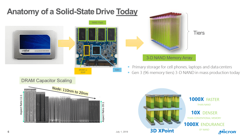
Anatomy of a Solid-State Drive gives details of new devices designed and assembled by Dr Gurtej Singh Sandhu. These Gen-3 (96 Memory Tiers) NAND Memory Arrays are used in Cell Phones, Laptops and Data Centres.